| 2023 | 
|
|---|---|
| 2022 | 
|
| 2021 | |
| 2020 |
|
| 2019 |
|
| 2018 |
|
| 2017 |

|
| 2016 |
|
| 2015 |

|
| 2014 |
|
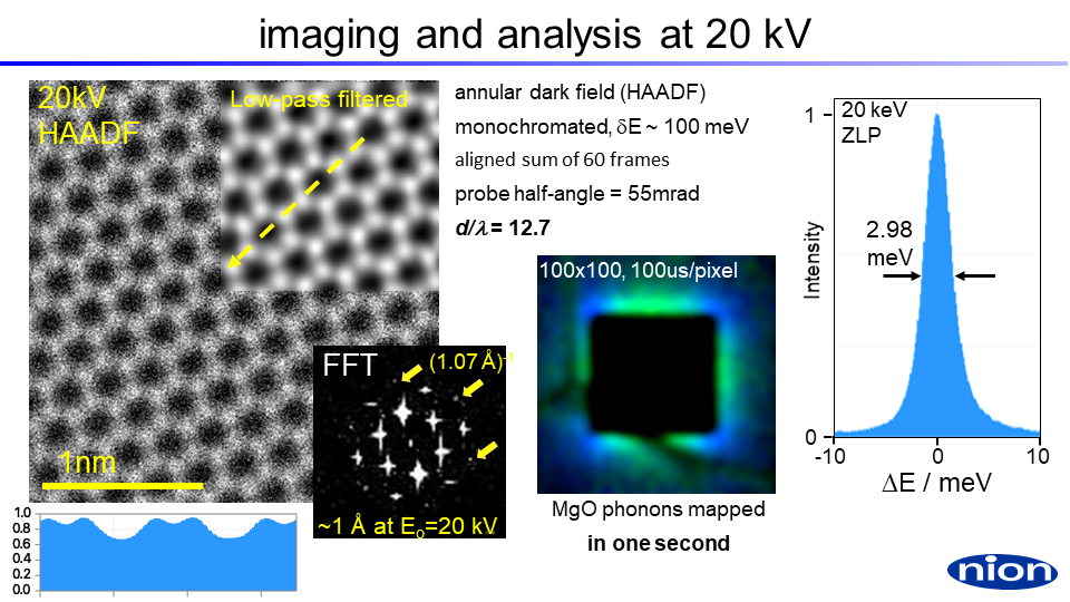
 The UltraSTEM™ 100 provides clear, atomic resolution imaging at reduced accelerating voltages. Examples of the resolving power at 60 kV are shown at left.
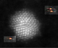
The top image is a high-angle annular dark field (HAADF) image of a multiply-twinned gold nanoparticle showing atomic columns. Insets (modified contrast) show individual gold atoms on the carbon substrate.
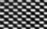
The lower panel shows an ADF image of silicon <110> crystal dumbbells, filtered to remove noise with spatial frequencies higher than those actually captured by the UltraSTEM™. It demonstrates that 1.36 Å resolution has been reached.
The UltraSTEM™ 100 provides clear, atomic resolution imaging at reduced accelerating voltages. Examples of the resolving power at 60 kV are shown at left.
The top image is a high-angle annular dark field (HAADF) image of a multiply-twinned gold nanoparticle showing atomic columns. Insets (modified contrast) show individual gold atoms on the carbon substrate.
The lower panel shows an ADF image of silicon <110> crystal dumbbells, filtered to remove noise with spatial frequencies higher than those actually captured by the UltraSTEM™. It demonstrates that 1.36 Å resolution has been reached.
Operating at 60 kV primary voltage greatly reduces radiation damage in materials containing low-Z elements such as B, C, N and O. Such materials include nanotubes, graphene and monolayer BN. The following images show a sequence of annular dark field (ADF) images (plus one BF image) of a single wall carbon nanotube recorded at 60 kV over about an hour, and ADF images of graphene and single-layer boron nitride. These results were collected using the ORNL UltraSTEM™ 100. They are described in greater detail in the Ultramicroscopy (2010) and Nature (2010) references given on the resources page.
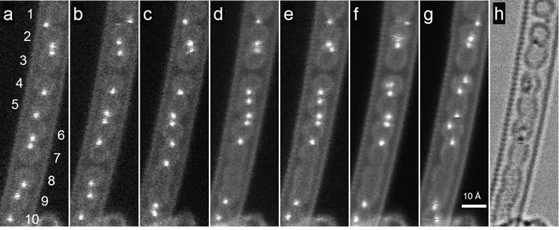 A series of unprocessed images of a single-wall carbon nanotube stuffed with C82 nanopods. Each nanopod initially contained one erbium atom, and these heavy atoms are imaged as bright dots. Note the gradual merging of the nanopods and the motion of the Er atoms between the nanopods. The top atom in nanopod 4 in frame (f) oscillates between two near-by positions.
Sample courtesy K. Suenaga, Ultramicroscopy, by permission.
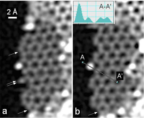 Single layer of graphene imaged about 2 minutes apart, and Fourier-filtered to remove shot noise and probe tails. One of the two 5-fold rings marked by single arrows in (a) and the single C dangling atom marked by the double arrow also in (a) have been replaced by a regular “armchair” configuration at the edge in (b). The inset profile of the heavier adatom at the edge reveals that it is probably Al.
Sample courtesy V. Nicolosi, Ultramicroscopy, by permission.
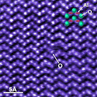
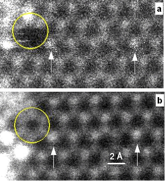 Unprocessed ADF images of the same area of monolayer BN. The dose used for image (a) was 4x lower than for (b), and the image is therefore statistically noisier. The BN hexagonal lattice consisting of alternating boron (darker) and nitrogen (brighter) atoms is readily distinguished, as are two substituting O atoms (marked by white arrows) which are brighter than N. The hole seen in (a) has become filled in (b), by C atoms. The heavier adatoms seen on the left are probably Na.
Sample courtesy V. Nicolosi, images courtesy M.F. Chisholm, Nature (supporting materials), by permission.
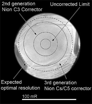 The Nion UltraSTEM™ at 100 kV is capable of sub-Å imaging by virtue of its 3rd-generation C3/C5 corrector. An experimental Ronchigram obtained in the UltraSTEM is shown below, demonstrating correction up to 40 mrad half-angle. The region in the center is the aberration-free region (sweet spot): electrons passing through it do not undergo excessive phase shift that would cause the STEM probe to blur.
Additional circles indicate the best sweet spot theoretically obtainable with the UltraSTEM correcting to 5th order (dashed); the sweet spot obtainable with Nion’s previous (C3-only) corrector; and the sweet spot of the microscope running with the corrector turned off.
 HAADF image of SrTiO3 taken at 100 keV with 320 pA probe current with 5 ms dwell time per pixel. The FFT (insert) shows that spacings of 1.23 Å (b) and 0.97 Å (a) were resolved.
Courtesy Cornell University.
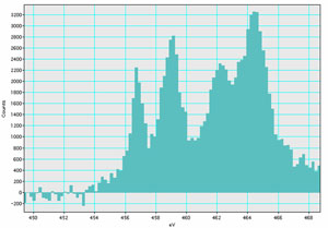 The UltraSTEM's high brightness gun and efficient detector coupling optics enable rapid acquisition of electron energy loss spectra. This is demonstrated in the following background-subtracted electron energy loss spectrum of the Ti L2,3 edge from a Ti column in SrTiO3.
The coupling optics collected angles up to about 50 mr half-angle into the Gatan Enfina parallel-detection spectrometer. Dispersion is 0.2 eV/channel and acquisition time is 0.5 sec. The splitting into four individual peaks is clearly resolved, and S/N ratio is excellent for the short acquisition time.
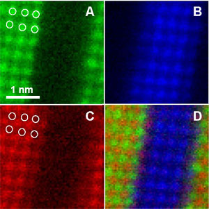 The high efficiency at collecting spectra means that the UltraSTEM can obtain elemental maps more rapidly than ever before. The images below are atomic resolution chemical maps of a La0.7Sr0.3MnO3/SrTiO3 multilayer showing La, Ti, and Mn composition at the interface (figs a, b, and c, respectively). These maps, when combined into composite RGB image (fig. d), elucidate the chemistry at the interface.
The green and red dots show that La and Mn occupy different columns in the La0.7Sr0.3MnO3layers. The red dots near the left interface indicate that Ti in the SrTiO3 layers occupies columns that are equivalent to those occupied by Mn in the La0.7Sr0.3MnO3 layers. Interestingly, in the composite image purple dots are visible at the interface between the two layers. This is evidence that, at this particular interface, there was a mixing of Ti and Mn within individual atomic columns.
The spectrum image was acquired using 40 mr illumination half-angle giving a 0.8 nA, 1.2 A probe. The EELS coupling efficiency was such that 0.6 nA of current entered the electron spectrometer. The high current allowed the acquisition of the 64x64 pixel map in only 29 s (7 ms per pixel) with 10 s of additional processing time.
Nion UltraSTEM 100. Courtesy Prof. D.A. Muller, L. Fitting Koukoutis and M.F. Murfitt, multilayer structure courtesy Drs H.Y. Hwang and J.H. Song.
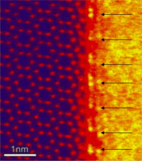 The < 1 Å probe available with the Nion Cs corrector enables direct interpretation of structure in interfacial studies. In the HAADF image to the left, two Si3N4 grains of differing orientation meet at an intergranular oxide film rich in lutetium (the right Si3N4grain is not oriented to the zone axis). Lu atoms at the boundary show a strong preference for specific sites at the terminating Si3N4 plane, resulting in a periodic structure in the intergranular film.
ORNL Cs-corrected HB603 (300 kV), courtesy N. Shibata and S.J.Pennycook.
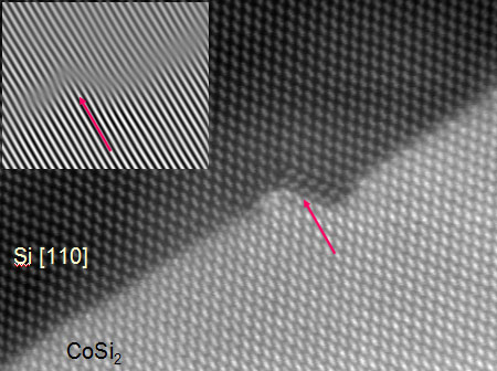 This image of a CoSi2 epitaxial layer on a Si [110] substrate shows a number of classic defect structures between two different interface types. The jog in the center contains a (-111) facet that has only a few layers arranged in a microtwin boundary. The crystal accomodates this with a misfit dislocation (arrowed).
The interface structure Si and disilicide crystal changes from a (1x1) structure on the left to a (2x1) reconstruction on the right. The reconstruction model of alternating ")(" shapes was previously proposed by Yu et al.,1 and was directly confirmed by this study. The inset shows the strain field for the interface structures, with dislocation indicated.
SuperSTEM 1 (100 kV), courtesy A. Bleloch.
 BF image of α-Al2O3 showing the characteristic zig-zags of the structure. A stacking fault of the (1120) type occurs in this crystal, where an extra zig-zag layer originating from the left terminates in a partial dislocation in the center of the image. The dislocation has a single O column at its core.
ORNL Cs-corrected HB603 STEM (300 kV), courtesy N. Shibata and S.J.Pennycook
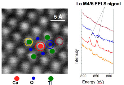 Single-atom chemical sensitivity is demonstrated in this HAADF image and electron energy loss spectra from CaTiO3 doped with La. The color-coded spectra on the right show the signal from individual atomic columns denoted by colored circles in the image. The red column has a strong La signal, which originates from a single atom of La within that column. The neighboring columns show a faint La signal due to slight delocalization of the probe, whereas the spectrum from two columns away shows no La signal.
ORNL Cs-corrected VG HB501 STEM, (100 kV), courtesy M. Varela and S.J. Pennycook.
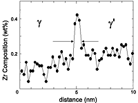 The figure at left shows an EDXS concentration profile of Zr across a grain boundary in a Ni-Cr-Fe alloy. The peak concentration of Zr at the grain boundary was only 0.3%, which means that the X-ray signal originated from fewer than 10 atoms.
Lehigh University Cs-corrected HB603 (300 kV), courtesy Masashi Watanabe
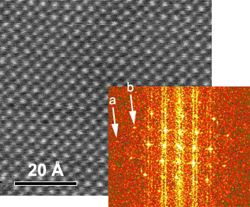
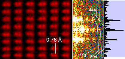 At higher energies, sub-Å imaging is readily achieved due to decreased contribution from chromatic aberration. This HAADF image of Si <112>, which has dumbbell spacing of 0.78 Å, was acquired at 300 kV. The Fourier transform of the image (right) shows transfer to 0.6 Å (804 spot).
ORNL Cs-corrected HB603 STEM (300 kV), courtesy M. Chisholm and P.D. Nellist.